VIA NEXT
Design for Testing
We provide:
Testability Design
Result Analysis and Summary
System Level Testing
Previous
Next
Design for Testing
Testability Design
With our structured and automated testing methodology, VIA NEXT can help easily detect any defects in your product’s IC design, ensuring your product is robust and fully standards compliant before reaching the market.
PKG
UBI
Mark
VMI
CP
FTH
FTC
SLT
FG
- Die Temp. @25°C
- Fault Coverage Test
- MFG ID
- Die Temp. @90°C
- Fault Coverage Test
- FTH_minV
- Max Power
- Guard Band(GB)
- PLL Calibration
- Speed Binning
- Per Part Database
- Die Temp. @5°C
- Fault Coverage Test
- FTC_minV
- Parallax Offset
- P/F@FTH_minV + GB
- Efuse
- Product ID
- Per Part Database
CP
PKG
FTH
UBI
FTC
Mark
SLT
VMI
FG
- Die Temp. @25°C
- Fault Coverage Test
- MFG ID
- Die Temp. @90°C
- Fault Coverage Test
- FTH_minV
- Max Power
- Guard Band(GB)
- PLL Calibration
- Speed Binning
- Per Part Database
- Die Temp. @5°C
- Fault Coverage Test
- FTC_minV
- Parallax Offset
- P/F@FTH_minV + GB
- Efuse
- Product ID
- Per Part Database
We provide:
- DFT test plan of logic ATPG & logic/memory BIST
- Stuck-at, functional, and speed fault coverage report
- Correlation analysis and report for coverage enhancement
- CP/FT Wafer test program development
- Probe card, load board, and active thermal control design
Design for Testing
Result Analysis and Summary
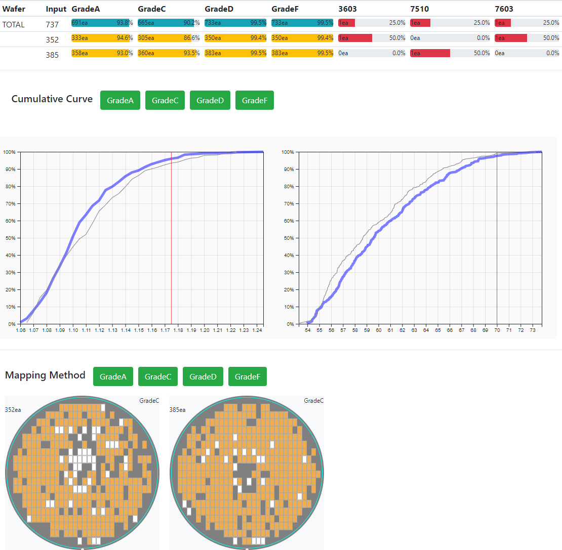
With our unique, proprietary DFT test circuit, VIA NEXT can easily aggregate and analyse IC testing data, allowing us to provide you with the data you need to improve your product’s design and yield.
Design for Testing
System Level Testing
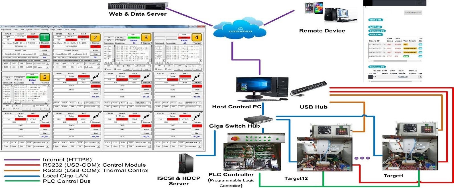
For more complex circuits which can’t be tested with fully automated tests, VIA NEXT can provide you with the capability to perform System Level Testing (SLT), allowing for direct test results at a lower cost.
We provide:
- SLT Board and Thermal Control Design
- Customized SLT Software Development
- Real-Time Monitoring of Test Results and Platform Status
- SLT Data Collection and Analysis


